Today, microLED display modules are made using a variety of wafer sizes for LED manufacturing after which the microLED wafer is bonded to an ASIC backplane (CMOS) wafer. The CMOS wafer is then cut down (cored out) to match the size of the epi wafer, wasting more than half of the CMOS wafer. COSTLY!!!
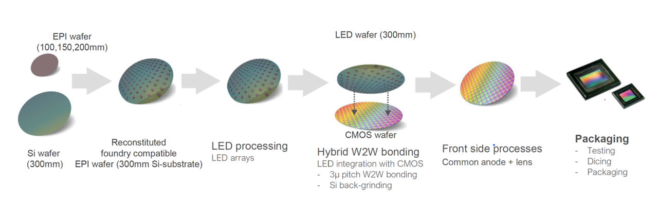
MICLEDI HIGH VOLUME MANUFACTURING FLOW
Using MICLEDI’s unique wafer reconstitution procedure, EPI starting material is diced and selectively placed on a 300mm silicon carrier wafer – no bow, no stress, known good epi die. The entire LED processing takes place in a world-class 300mm production wafer flow for low-cost mass production. Industry standard or customized CMOS backplane wafers are hybrid bonded to MICLEDI’s LED wafer, then diced, packaged, tested, yielding fully integrated microLED display modules without ever having to discard portions of the CMOS ASIC backplane wafer.
FULLY INTEGRATED MICROLED DISPLAYS
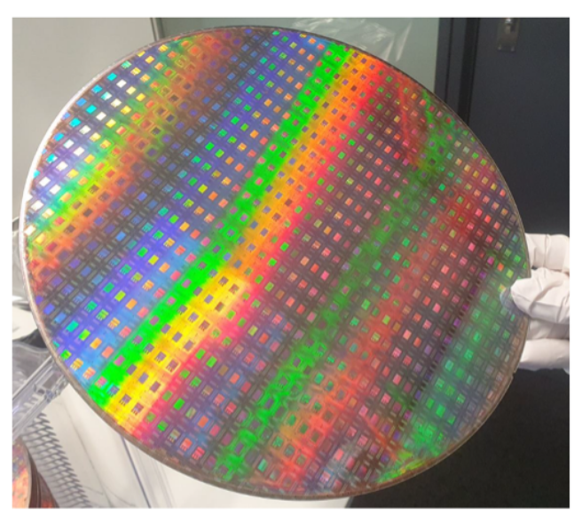
Beautifully planarized, MICLEDI’s 300mm reconstituted “epi wafer on standard silicon” boasts nearly 100% die attach yield. Using all high-precision photolithography equipment readily available in world class 300mm CMOS foundries, MICLEDI’s microLEDs capitalize on many of the manufacturing practices that have been in common use making backside illuminated imagers in high volume. Proven methods translate into no wafer breakage due to stress during LED processing, predictable performance, and high yields.